





Fragmented IP catalog
Internal and third-party IP scattered across repos, spreadsheets and vendor portals — no single source of truth.
Glide Semi unifies semiconductor IP Management and Operations BoM Management in a single, integrated platform. Design outputs flow straight into wafer, packaging, assembly and test — with your engineers never leaving the tools they already use. No throw over the wall.
 Engineers stay in their tools — zero extra workIP + Operations BoM, one platformGDSII → Wafer → Package → Tested Chip
 Live traceability
 Controller IPinternal wrapper
 Substratesourcing
 DesignRTL → GDSII
 Waferfoundry
 Packageassembly · test
 Qualified chipship-ready
 Silicon
Adoption dies when a platform asks engineers to enter data twice. Glide Semi never does. Designers stay in their EDA cockpit, RTL teams stay in Git or Perforce, ops stays in PLM/ERP — Glide listens to the systems of record they already use and assembles the connected picture underneath them.
No second system to update — signals are captured from tools of record No new workflow imposed on design, verification or operations Milestones, dependencies, IP usage and BoM changes flow in automatically The connected view is assembled for your teams, not by them
Glide Sits Above Your Stack — it assumes your Git, Perforce and EDA hygiene already exist, and adds the connective layer on top rather than replacing anything.

 Glide Semi captures the signal automatically
milestones · dependencies · IP usage · BoM changes — no new data entry


The wall between design and operations is where schedules slip and yield surprises hide. Glide Semi removes it: GDSII isn’t thrown over a fence — it’s a governed hand-off on the same platform that carries the wafer through packaging, assembly, test and qualification.

 Project Mgmt
 Requirements
 Design/EDA
 IP Management
 MES
MES ERP
ERP Sourcing
No More Throw-Over-The-Wall. Project management, requirements, design/EDA, IP management, MES and ERP operate as one integrated platform — so a change in design is visible to operations, and a constraint from the fab or OSAT is visible to design, in the same place.
 GDSIItapeout DB
 Mask / Foundrywafer fab
 Wafer Sortprobe · bin
 Assemblydie attach · bond
 Packagingsubstrate · mold
 Final TestATE · burn-in
 Qualified ChipJEDEC / AEC-Q
When design signs off GDSII, the work isn’t done — it’s handed to operations. Glide carries that hand-off natively: the tapeout database feeds mask and foundry, the wafer moves through sort, assembly, packaging and final test, and the operations BoM (die, substrate, materials, package) is managed on the same platform as the IP that produced it.
GDSII / tapeout database governed as the design-to-ops hand-off artifactOperations BoM — die, substrate, bond, package, materials — beside the IP BoMInherent Qualifications Tracked: Process, Package, Assembly And Test QualBonding diagrams, package drawings, material specs and test specs anchored to the SKUSourcing network managed — foundry, OSAT, substrate, test house and materialsGlide Semi is the connective tissue across the systems that run a semiconductor business. It integrates project management, requirements management, design/EDA tools, IP management, MES and ERP so that a single thread of truth runs from a requirement, through the IP that satisfies it, to the wafer and unit that ship against it.
Requirements trace to the IP and silicon that fulfil themDesign/EDA milestones and MES lot events on one timelineERP sees IP licensing and BoM cost; operations sees design intentProvider-agnostic connectors — sits above the tools, replaces none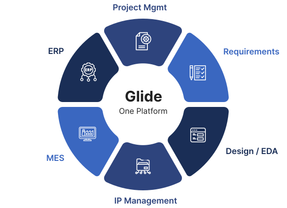
Every IP block, wrapper, license, GDSII drop, wafer lot, package and SKU is interconnected. When one thing changes, the impact propagates across programs and across the design-operations boundary. Reconstructing that by hand doesn’t scale.
Internal and third-party IP scattered across repos, spreadsheets and vendor portals — no single source of truth.

Teams cannot see every program, wrapper, vendor drop and downstream operation affected by one change.

GDSII gets thrown over a fence; packaging, assembly and test constraints surface too late to act on.

Per-use, per-program and royalty terms live in contracts — not where engineers design-in.

Foundry, OSAT, substrate and test dependencies are not linked to the design that relies on them.

Impact analysis becomes a manual spreadsheet exercise that relies on memory and does not scale with reuse.

Glide Semi sits above your existing tools and models what they can’t: the relationships between IP, programs, licenses, vendors, sourcing and silicon.
A unified catalog for every MAKE and REUSE block — versions, ownership, lifecycle state and technical milestones from spec-freeze to tapeout-ready.
Model licensed vendor blocks and the internal wrapper that consumes them — external and internal IP kept cleanly, explicitly distinct.
Per-use, per-program, royalty, subscription and perpetual models — with entitlements, scope, pricing and a live programs remaining position.
Structured decisions for every block — cost, schedule, risk and reuse — that become a tracked BoM line, not a lost slide.
Bring IP vendors into the loop — deliveries, spec conformance, errata and version drops flow to the wrapper and fan out to every consumer.
Provider-agnostic: Git, GitLab, Perforce, Gerrit. Milestones and results push in; dependency gates and CI triggers push back out.
One transaction pattern for every request — new IP, change, waiver, retirement — with request → promise → work → accept and full audit.
A defect is the master record; vendor errata and internal finds are sources; wrapper mitigation and vendor fixes are independent resolutions.
Operations BoM, bonding diagrams, material specs, package drawings and datasheets — each anchored to the IP, program or product it governs.
Every internal IP is something you build (MAKE) or a wrapper around something you license (BUY). Glide models both layers explicitly — and meters real usage against the license so over-use and expiry surface before they become exposure.
Track what you own and what you license in a single portfolio, with the wrapper relationship first-class. When a vendor ships a new drop, Glide knows exactly which wrapper — and which programs — are affected.
MAKE blocks, REUSE blocks and BUY wrappers in one lifecycleVendor block and its wrapper kept distinct — never conflatedMulti-vendor wrappers: one internal IP integrating several licensed blocksLicense covers the block · wrapper consum
 Per-program
 Per-use
 Royalty/unit
 Subscription
 Perpetual
 Site/enterprise
Manufacture · per-program · max 3
A 4th program is blocked → escalate to amend the license
Model any commercial arrangement — per-use, per-program, royalty, subscription, perpetual, site or enterprise — with entitlements, scope, pricing and obligations. Entitlement checks gate design-in, so a program that would exceed the license is stopped and escalated.
Live “programs / units remaining” and expiry alertsRoyalty Accrual On Shipment, With Vendor-Ready Usage ReportsTerritory, Field-Of-Use, Node, Foundry And Exclusivity ScopeThe operational backbone that turns a catalog into a managed portfolio.

Vendors are first-class actors. Delivery acceptance, spec conformance, re-synthesis, DRC confirmation and export clearance each drive the internal wrapper’s state — and every vendor milestone emits a paired internal-IP consequence, linked back to its trigger.

One defect record is the master; vendor errata and internal finds are its sources; the vendor fix and the wrapper mitigation are two independent tracks that must both complete to close. “Fix released” is not “resolved.”

New IP, change, waiver, retirement — every request is the same transaction: request and promise, the type-specific work, then an explicit accept. One workspace, configured per type, fully auditable.
From make-vs-buy through GDSII to a tested, qualified chip — every stage connected, every change traceable to the IP, license, program and sourcing it touches.

Make-vs-buy analysis; IP request raised; BoM line created.

External IP licensed; vendor drop accepted into the wrapper.

Spec -> RTL -> verification, from SCM.

DRC/LVS clean -> GDSII hand-off governed into operations.

Foundry, sort, assembly, packaging and final test with qualification.

Royalty accrues on shipment; vendor usage reports generated.
Built Bottom-Up For Silicon — From The IP Graph, Change Propagation And The Design-To-Operations Flow, Not BOM Governance Borrowed From Mechanical PLM.
blast-radius on every change
platform for IP + operations
extra work for engineers
design-to-ops wall
time-to-market
GDSII-to-chip traceability
cost of errors & rework
impact analysis, not reconstruction
 Git
Git GitLab
 Perforce
 Gerrit
 Jira
Jira Jama
Jama EDA flows
 MES
MES ERP
ERP
